Sketching Circuits: Schematics and Perfboard Layouts on Graph Paper
Most circuits get drawn twice before anything is soldered: once as a schematic, which says what connects to what, and once as a layout, which says where each part physically goes. Both are faster on paper than in software, and one particular ruling makes the second one close to automatic. Ten squares to the inch puts a line every 0.1 inch, and 0.1 inch is the pitch of a breadboard hole, a perfboard hole, a stripboard hole and the pins of every through-hole integrated circuit ever made. That is not a rough match. One square is one hole, at full size, so a layout drawn on the paper transfers to the board by counting rather than by measuring. This article covers how to set the sheet up, how symbols and wires land on the grid, how to get from a schematic to a working layout, and the parts of modern electronics where the rule does nothing for you at all.
Why 0.1 Inch Changes Everything
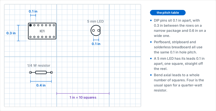
Through-hole electronics was standardized on a tenth of an inch decades ago and never moved. The pitch survived the transition to metric documentation as 2.54 mm, an exact conversion rather than a rounded one, and it is still what you get when you buy a strip of headers, a solderless breadboard or a bag of DIP sockets. That single number is why engineering graph paper is a drafting tool for electronics rather than just a convenient surface.
Print a sheet at ten divisions to the inch and you have a full-size map of a board you have not built yet. Count four squares between two holes on the paper and a quarter-watt resistor with its leads bent to 0.4 inch drops straight in. Count three squares across and a narrow DIP package straddles them exactly. Nothing has to be scaled, converted or trusted.
The Numbers That Matter
Four dimensions cover almost everything you will lay out by hand, and all four are whole numbers of squares:
| Part | Dimension | Squares |
|---|---|---|
| DIP pin pitch | 0.1 in (2.54 mm) | 1 |
| DIP row spacing, narrow body (8 to 20 pins) | 0.3 in | 3 |
| DIP row spacing, wide body (24 pins and up) | 0.6 in | 6 |
| 5 mm LED lead spacing | 0.1 in | 1 |
| Quarter-watt axial resistor, leads bent | 0.4 in | 4 |
| Ceramic disc capacitor | 0.1 or 0.2 in | 1 or 2 |
| Perfboard, stripboard, breadboard holes | 0.1 in | 1 |
The one part that regularly catches people out is the TO-92 transistor, the small plastic half-cylinder used for signal transistors and voltage regulators. Its three leads leave the package 0.05 inch apart, half a square, and have to be splayed into a 0.1 inch triangle or an in-line 0.1 inch spread before they will meet a board. Draw the footprint you intend to use, not the pin spacing on the part in your hand.
Inches, Not Millimeters
This is the one place on the whole site where the imperial setting is not a preference. A 2.5 mm metric rule looks close enough to 0.1 inch and is not: 2.54 mm against 2.5 mm is a 1.6 percent error, which is invisible over one square and is 1.6 mm by the time you have counted forty holes across a board. Halfway along a long DIP the pins are visibly off their holes and the drawing has stopped being a template.
So set the generator to imperial and ten divisions per inch before anything else, and print at 100 percent with page scaling off. Our printing tips guide covers the driver settings that quietly resize a page; on this particular job a sheet printed at 96 percent is not slightly wrong, it is useless. Check a fresh sheet with a ruler across ten squares before you draw on it. If it measures an inch, the rest of the work is safe.
Drawing a Schematic on the Grid
A schematic is a diagram of connections, not a picture of a board. Nothing on it is to scale and nothing needs to be, which is exactly why the grid helps: it takes care of straightness, spacing and right angles so your attention stays on the circuit.
Symbols Sized in Squares
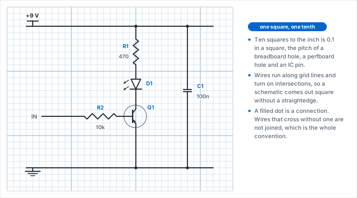
Pick a size for each symbol in whole squares and use it everywhere on the sheet. A resistor drawn six squares long, with one square of lead at each end and the zigzag across the middle four, is a good starting point; every resistor on the page then looks identical and the eye stops having to check. A capacitor is two plates a third of a square apart across the wire. A diode or LED is a triangle a square and a half tall pointing the way the current flows, with the cathode bar across its tip. A transistor gets a circle roughly three squares across with its base bar down the middle.
The discipline is not aesthetic. Symbols drawn at a consistent size are recognized without being read, which is what lets you follow a circuit you drew last month, and it is the same reason a grid method drawing keeps proportion under control. Vary the sizes and every symbol has to be identified individually.
Wires, Corners and Junctions
Wires run along grid lines and turn only at intersections. Diagonals are legal but almost never worth it: a schematic made entirely of horizontals and verticals is far easier to trace, and the grid gives you both for free.
Junctions follow one convention that has not changed in fifty years. A filled dot at an intersection means the wires are connected; two wires crossing with no dot are not. Because a dot can be missed or added by a smudge, the practice worth adopting is to avoid four-way junctions entirely: where four wires meet, offset them into two three-way tees a square apart. Then a connection is unambiguous even on a photocopy, and there is no crossing on the page that could be misread as a join.
Give power and ground their own horizontal rails across the top and bottom of the sheet and drop every branch between them. It costs a little space and it removes most of the wire crossings you would otherwise have to draw.
Designators and Values
Every part gets a reference designator and a value, and both need somewhere to sit. The letters are standardized: R for resistors, C for capacitors, D for diodes and LEDs, Q for transistors, U or IC for integrated circuits, SW for switches, J for connectors. Number them in the order you draw them and never reuse a number, even for a part you delete.
Put the designator on one side of the symbol and the value on the other, both parallel to the wire, and keep them in the same relative position all over the sheet. Values use the standard shorthand: 470R or 470 ohms, 10k, 2M2 for 2.2 megohms, 100n for 100 nanofarads, 10u for 10 microfarads. Writing the multiplier in place of the decimal point, so 2k2 rather than 2.2k, exists precisely because a decimal point does not survive a photocopy or a smudge.
Choosing the Ruling
Here is the split that catches most people: the ruling that is perfect for a layout is too fine for a schematic. On a layout every square has to be a real hole, so ten to the inch is fixed. On a schematic nothing is to scale, and the constraint is your handwriting, which does not get smaller when the grid does. A designator and a value written at normal size beside a six-square resistor need roughly a quarter of an inch of height each. At ten squares to the inch the labels are larger than the symbol they belong to.
| What you are drawing | Ruling | Why |
|---|---|---|
| Perfboard or stripboard layout | 10 squares per inch | One square is one hole, at full size |
| Solderless breadboard planning | 10 squares per inch | Same pitch, same 1:1 transfer |
| Schematic drafting | 4 or 5 squares per inch | Room for symbols, designators and values |
| Block diagrams and signal flow | Quarter inch, or dot grid | Alignment only; a printed grid is a distraction |
| Frequency response and gain plots | Semi-log | Decades, not equal squares |
| Enclosure and front panel drilling | 10 squares per inch | Hole centers counted rather than measured |
The practical answer is to print two rulings and keep both in the drawer. Draw the schematic at five to the inch where there is room to write, then lay the board out at ten to the inch where every square counts. If you are unsure how a ruling will feel before you commit a stack of paper to it, our guide to choosing the right grid size works through the same trade-off for other kinds of work.
A dot grid is worth trying for schematics if printed lines bother you. The dots mark the same intersections, so wires and symbols still land consistently, but a finished drawing photographs as a clean circuit on near-white paper instead of a circuit inside a cage.
From Schematic to Perfboard Layout
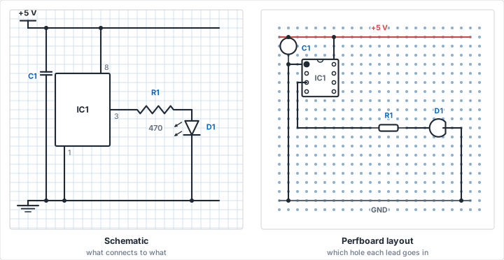
Perfboard is a sheet of insulator drilled on a 0.1 inch grid, each hole with its own isolated pad. It makes no connections for you, which means the layout is entirely yours to plan, and planning it on paper first is the difference between a board that works and an afternoon spent with a solder sucker.
Place the Integrated Circuits First
Start with the largest, least movable parts. An IC occupies a fixed block of holes and everything else arranges itself around it, so place those before anything else, leaving a clear square or two around each package for the wires that have to reach it. Orient every IC the same way up if you can. Pin 1 in a consistent corner across the whole board means you never misread a pin number while soldering, and it makes the board legible to anyone else.
Then place the parts that have to be somewhere specific: connectors at the board edge, adjustable components where a screwdriver can reach them, indicator LEDs where they will show. Decoupling capacitors go across the supply pins of the IC they belong to, not somewhere convenient. Everything left over is genuinely free.
Route the Nets
Work through the schematic one net at a time, marking each on the schematic as you commit it to the layout so nothing gets drawn twice or forgotten. Run power and ground first, as long buses along the top and bottom of the board, exactly as on the schematic. They connect to the most parts, so giving them the straightest runs saves the most wire.
Everything else routes between them, along lines of holes with square corners. Where two nets have to cross, one of them can hop over on an insulated jumper on the component side, which is the perfboard equivalent of a via and worth marking on the drawing so you do not forget to fit it. Count the holes for every wire and write the count down; that number is your cut length, and cutting wire to a counted length is much faster than offering each piece up to the board.
The Mirror Problem
This is the one mistake that reliably ruins a first perfboard build. You draw the layout looking at the component side, because that is where the parts are and where the drawing makes sense. You solder looking at the other side, where everything is reversed left to right. Pin 1 of the IC, which was top left on your drawing, is now top right on the board in front of you.
There are three defenses and you should pick one deliberately. Mark the drawing COMPONENT SIDE in the corner and consciously flip every reading, which works and is the most error-prone. Draw the layout twice, once from each side, which is the traditional answer and takes ten extra minutes. Or draw it once on tracing paper or vellum and simply turn the sheet over, which gives you a correct mirror image at no cost and no risk of the two drawings disagreeing. Whichever you choose, label every drawing with the side it represents before you put the pen down.
Stripboard Changes the Rules
Stripboard, often called Veroboard, uses the same 0.1 inch hole grid but joins the holes with continuous copper strips running the length of the board. That changes the layout problem completely. On perfboard you draw the connections you want; on stripboard the connections already exist and you draw the cuts that remove the ones you do not.
A stripboard layout therefore needs two kinds of mark on the same sheet. The strips run along one axis, so shade or line every row of the grid that corresponds to a copper strip and keep parts and links on the squares as usual. Then mark each break with a distinct symbol, conventionally a small cross or a filled circle on the hole where the track is cut, because a break is made at a hole rather than between two. A dedicated spot-face cutter or a 3 mm drill bit turned by hand does the cutting.
Two habits prevent almost every stripboard fault. Count the breaks on the drawing and count them again on the finished board before you fit any parts, since a missed cut is a short you will chase for an hour. And place a DIP so it straddles a gap you have already broken under the package, because the two rows of pins are on different strips and the strips must not run between them.
Breadboarding from the Same Sheet
A solderless breadboard is the same grid again, with the holes already connected in short groups. Five holes in a column form one node, the two halves of the board are separated by a center channel exactly 0.3 inch wide, and that width is not arbitrary: it is the row spacing of a narrow DIP, so an IC straddles the channel with each row of pins in its own set of nodes. The long rails down the sides are the power buses.
Draw the board as a grid of holes and outline the node groups, and a breadboard layout becomes something you can plan away from the bench and check before you build. It also gives you a record. A working breadboard that has been taken apart is gone, whereas a sheet with every node marked can be rebuilt in ten minutes or turned straight into a perfboard layout using the same squares.
Where Graph Paper Stops Helping
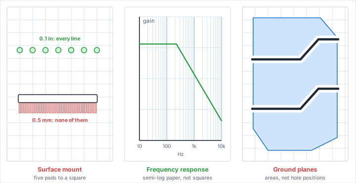
The rule works because through-hole parts are built on a tenth of an inch. As soon as something is not, the paper is at best neutral and at worst misleading.
Surface-mount parts are the clearest case. A fine-pitch package puts its pads 0.5 mm apart, which is about one fifth of a square, so five pads land inside every square and none of them on a line. Drawing an SMD footprint on a 0.1 inch rule gives you a picture that is wrong in a way that looks right, which is worse than freehand. The same goes for anything measured in fractions of a millimeter: trace widths, clearances, drill sizes.
Anything about copper as an area rather than as a position is also off the rule. Ground planes, pours and their clearances are defined by how far the copper has to stay from everything else, and no line of the grid predicts where that boundary falls. And measurements plotted against frequency belong on logarithmic graph paper, where a decade of frequency occupies a fixed distance and a single-pole roll-off is a straight line; on equal squares the same curve is unreadable at one end and empty at the other. Our guide to graphing lab data covers axis choice and best-fit lines for bench measurements of that kind, and the mathematics graphing tutorial covers setting up scales from scratch.
The honest summary is that paper carries a through-hole board of maybe a few dozen parts extremely well, and stops there. Past that point the net count exceeds what you can track by hand, and the right move is to keep the paper for the schematic and the thinking and let software handle the routing.
Mistakes That Cost You a Board
Mistake: The Sheet Printed at 97 Percent
Problem: The printer driver defaulted to fit-to-page, so the squares are close to a tenth of an inch and not quite. The layout looks fine, the first two parts fit, and the far end of a 16-pin DIP misses its holes by most of a hole width.
Solution: Print at 100 percent with scaling off, then check a fresh sheet with a ruler across ten squares before you draw. It should measure exactly one inch. This takes five seconds and it is the only check that matters.
Mistake: Laying Out on a 2.5 mm Metric Rule
Problem: Metric paper was to hand and 2.5 mm looked like a tenth of an inch. It is 1.6 percent short, so the error accumulates: invisible over one square, over a millimeter by the twenty-fifth hole, and enough to put a long package off its pads.
Solution: Set the generator to imperial for any layout work. Metric rules are fine for schematics, where nothing is to scale, and wrong for anything that has to map onto real holes.
Mistake: Soldering from a Component-Side Drawing
Problem: The layout was drawn looking at the parts and the board is being soldered from the other side. Every position is mirrored, and pin 1 ends up diagonally opposite where it belongs. It usually goes unnoticed until the board is powered.
Solution: Label every layout drawing with the side it shows, and produce the mirrored version rather than trying to flip it in your head. Drawing on tracing paper and turning the sheet over gives you both views from one drawing.
Mistake: The Four-Way Junction
Problem: Four wires meet at one intersection with a dot on it. Scanned, photocopied or drawn in a hurry, the dot is ambiguous, and nobody reading the schematic can tell a crossing from a connection.
Solution: Never join four wires at a point. Offset them into two three-way tees one square apart. The circuit is identical and the drawing can no longer be misread.
Mistake: Leaving No Room Around the ICs
Problem: The layout is packed to get the board as small as possible, and then three wires need to reach the same side of a package with nowhere to run. The board grows anyway, in the worst possible way, with links crossing over the top of parts.
Solution: Leave a clear square or two around every IC before routing anything. Perfboard is cheap and your time is not; a board an inch wider is a better outcome than a mat of jumpers.
Conclusion
Ten squares to the inch is not a convenient approximation for electronics work, it is the actual dimension the hardware was built on. That makes a printed sheet a full-size template rather than a sketch surface: parts are placed by counting holes, wires are cut to a counted length, and a layout transfers to a board without a single measurement being taken. For a through-hole project of a few dozen parts it is quicker than any software, and it leaves you with a record you can still read in a year.
Print two rulings and use them for different jobs. Five to the inch for schematics, where your handwriting sets the scale and the symbols need room to breathe. Ten to the inch for layouts, where the paper is standing in for the board. Keep the imperial setting for anything that has to land on real holes, label every layout with the side it shows, and let the grid do the straightening while you think about the circuit.
Print 0.1 Inch Engineering Paper
Set the units to imperial, choose ten divisions per inch, and print at 100 percent with scaling off. Free, with no account and nothing to install.
Create Engineering Graph PaperRelated Resources
- Engineering Graph Paper -- the ruling this whole article runs on
- Dot Grid Paper -- the same intersections without the printed cage
- Logarithmic Graph Paper -- semi-log sheets for frequency response
- Graphing Science Lab Data -- plotting what the bench actually measured
- Woodworking and DIY Project Plans -- drilling an enclosure to the same counted grid
- Design Sketching on Graph Paper -- sketching the case the board goes into
- Mathematics Graphing Tutorial -- setting up axes and scales
- Back-to-School Graph Paper -- what to print at the start of a term